by
John R. Fischer, Senior Reporter | February 23, 2021

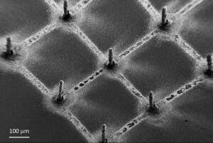
Using aerosol jet-printing, the researchers 3D-printed affordable, high-resolution X-ray detectors that improve scanner performance and reduce radiation exposure
Scientists at the School of Basic Sciences in Switzerland’s École polytechnique fédérale de Lausanne (EPFL) have 3D-printed cost-effective, high-resolution X-ray detectors that can be integrated into standard microelectronics to improve performance and reduce radiation exposure in medical imaging scanners.
They used aerosol jet-printing, a new 3D-printing technique used to manufacture electronic components. The materials used to make the detectors were graphene and perovskites, which may help to decrease required X-ray doses for forming an image by more than a thousand times, according to Dr. Endre Horváth, scientific assistant of InSTI-HEPIA and guest scientist at LQM-EPFL.
"Lead halide perovskites are soluble in various solvents which is a great advantage for printing based techniques to apply for future industrial production of solar cells, LEDs and various detectors based on this peculiar semiconductor. This family of materials contain heavy elements such as lead and iodine that have a large X-ray scattering cross section, one of the basic requirements to create high-sensitivity X-ray detectors."


Ad Statistics
Times Displayed: 2147
Times Visited: 10 Fast-moving cardiac structures have a big impact on imaging. Fujifilm’s SCENARIA View premium performance CT brings solutions to address motion in Coronary CTA while delivering unique dose saving and workflow increasing benefits.
Medical imaging scanners often work with low-exposure conditions, which requires high-resolution detectors that can operate at a low photon flux. Photon flux refers to how many photons hit the detector at a given time and determines the number of electrons it generates as a result.
With aerosol jet printing, the researchers 3D-printed perovskite layers on a graphene substrate, with the perovskite acting as the photon detector and electron discharger, while the graphene amplified the outgoing electrical signal. They chose graphene and perovskites due to their being versatile and easy to synthesize, and because perovskite has heavy atoms that provide a high scattering cross-section for photons. They also used methylammonium lead iodide perovskite (MAPbI3), which holds optoelectronic properties that pair well with its low fabrication costs.
The detectors were found to have record sensitivity and created a fourfold improvement in best-in-class medical imaging devices. They also made it simple to form images, according to said lead scientist professor László Forró.
"It doesn't need sophisticated photomultipliers or complex electronics," he said in a statement. "This could be a real advantage for developing countries."
Further research is required according to Horváth. "For medical imaging, more pixels should be fabricated on a larger surface. CT scans use higher X-ray energies than the 8 KeV source employed in this work, so we need to repeat the measurements for 100 keV photons to confirm the device’s suitability for medical applications. The pixel-to-pixel reproducibility and the most efficient signal reading has to be studied, and we need to work on the reduction of the dark current too."
An EPFL patent has not been granted and may allow for further industrialization efforts. Coming up with a turn-key solution and validating it in clinical care will require industrial partners, says Horváth.
The scientists’ work was published in
ACS Nano.

